The exposed surface of a conventional resistive sensor is flexible film. That enables force activation but may not suit repeated abrasion or aggressive cleaning. G/F/G adds a thin, chemically strengthened micro-glass layer over the resistive film.
Mildex can coordinate that surface with the resistive sensor, optical adhesive, sunlight-readable options, EMI shielding, controller, bonding, LCD, and mechanical design.
Inside the G/F/G material stack

- Micro-glass surfaceChemically strengthened glass faces the user.
- Optical adhesiveBonds the micro-glass to the resistive film.
- PET filmFlexible film carries the upper electrode.
- Upper ITO coatingConductive coating on the underside of the film.
- Spacer dots and air gapMaintain separation until force closes the contact.
- Perimeter tape (DST)Joins the sensor around its perimeter.
- Lower ITO coatingConductive coating on the glass substrate.
- Glass substrateRigid support for the lower electrode.
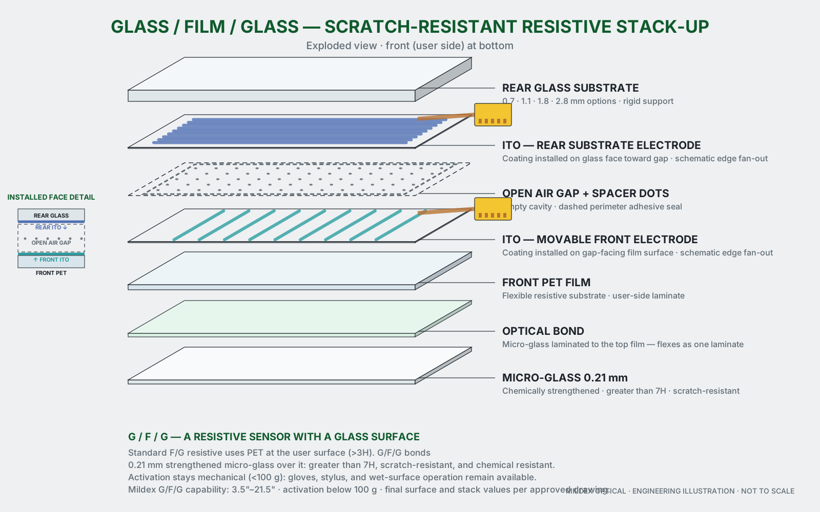
Diagram, simplified for mobile
- 0.21 mm micro-glass becomes the user surface
- Optical adhesive joins it to the movable resistive film
- Spacer dots preserve the force-activated air gap
- The ITO glass substrate completes the sensor
How glass is added without losing resistive activation
The micro-glass is optically bonded to the flexible top film. At the published thickness it can move with the film under applied force, allowing the upper and lower conductive layers to make contact.
The sensing method therefore remains force activated. Gloves, passive stylus, wet-surface operation, and in-assembly shielding can remain available while the operator touches a glass surface.
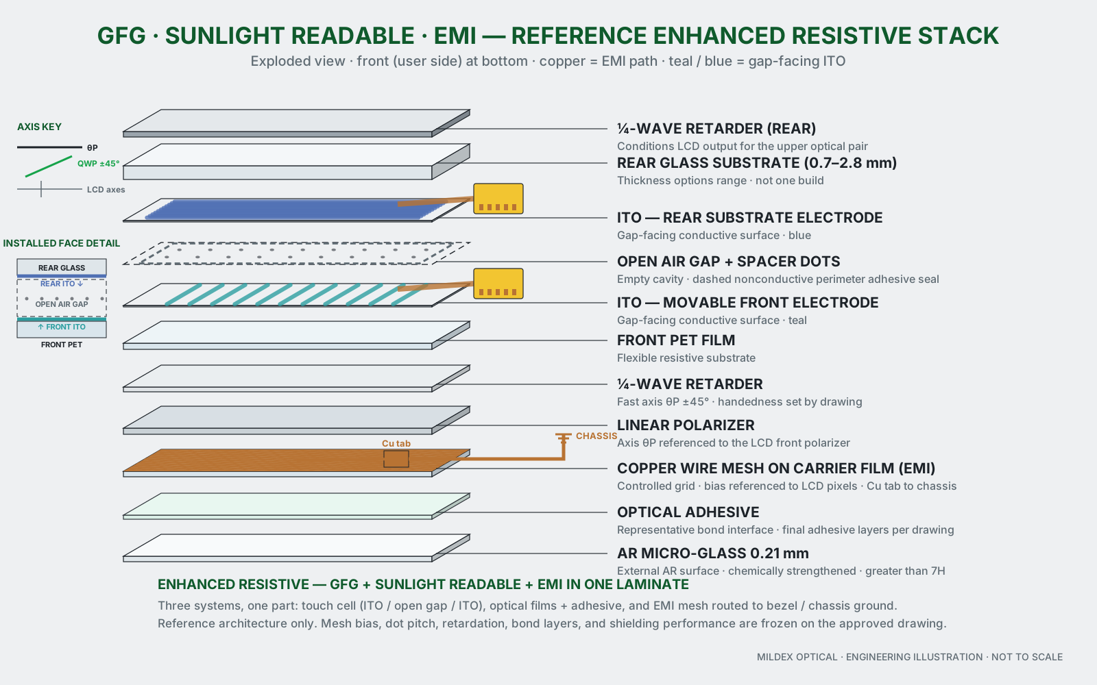
Diagram, simplified for mobile
- Base: G/F/G force-activated sensor
- Optical option: sunlight-readable polarizer films
- EMI option: conductive shield with a defined enclosure-ground path
What Mildex can coordinate around G/F/G
- User surface. Micro-glass, hardness, impact, abrasion, cleaning and chemical exposure.
- Touch behavior. Activation force, glove, stylus, wet operation, controller, cable, and interface.
- Optical options. Clear, AR, AG, anti-smudge or related surface systems, sunlight-readable films, and bonding to the LCD.
- EMI design. Conductive mesh or coating, bias angle, perimeter connection, cable and enclosure-ground path.
- Complete assembly. Sensor construction, LCD, bonding, mechanics, environment, and functional testing.
Why surface durability must be designed with the sensor
Adding a harder surface changes force transmission, optics, adhesive behavior, edge construction, thickness, weight, and mechanical loading. Mildex can evaluate the surface and resistive sensor as one construction rather than leaving the OEM to combine unrelated parts.
Published G/F/G capability envelope
| Parameter | Mildex capability data |
|---|---|
| Micro-glass | 0.21 mm, chemically strengthened, optically bonded |
| Surface hardness | >7H / Mohs 5 |
| Sizes | 3.5–21.5 in |
| Interfaces | 4-, 5-, 8-wire and RMTS |
| Position accuracy | 98.5% |
| Activation force | <100 g |
| Coatings | Clear, AR, AG, AS, MAR, and combinations |
| EMI option | 0.25 or 5 Ω/sq, Class B |
| Transmission by stack | 78–80% GFG; 74–76% +SR; 75–77% +EMI; 72–74% +SR+EMI |
| Operating / storage | −30 to +80 °C operating / −40 to +85 °C storage, depending on stack-up |
Published values describe product-family constructions. Confirm the exact micro-glass, sensor, adhesive, optical films, coating, controller, shield, ground path, bond, LCD, temperature range, and test method on the released drawing.
When G/F/G may not be the best starting point
Standard film/glass resistive may be simpler where abrasion and aggressive cleaning are limited. PCAP with strengthened cover glass may fit better when a seamless printed lens and capacitive multi-touch define the interface.
Panel selection guide
Start with the surface exposure and input method.
Use the guide to capture cleaning chemistry, abrasion, glove, stylus, wet operation, screen size, brightness, environment, EMI, and integration level.